Skip to content
Odtutor
NEET Preparation
NEET Physics
NEET UG Physics Practice Paper – Set 15 (Nuclei +...
NEET UG Physics Practice Paper – Set 14 (Dual Nature...
NEET Biology
Unit – 3 Cell Structure and Function – NEET Biology...
Salient features and classification of animals – Notes for Unit...
NEET Chemistry
NEET UG – Chemistry Practice Paper Part 21 | Topic:...
NEET UG – Chemistry Practice Paper (Previous Years’ Questions) Part...
IIT-JEE Preparation
IIT JEE Chemustry
IIT JEE Chemistry Practice Paper – Part 18: Ionic Equilibrium...
IIT JEE Chemistry Practice Paper – Part 17: Solutions &...
IIT JEE Chemistry Practice Paper – Part 16 (Thermodynamics) with...
IIT JEE Maths
IIT JEE Maths Practice Paper 20 – Matrices and Determinants...
IIT JEE Maths Practice Paper – 19 – PYQs- focused...
IIT JEE Maths Practice Paper – 18 – PYQs –...
Bank Exams
Arithmetic Aptitude >>
Clock Aptitude Problems: Tips and Tricks to Solve in IBPS...
Calendar Aptitude Problems: Tips and Tricks to Solve in IBPS...
Career
Student Registration
Dashboard
Log In
All Articles
Simulators
Resistance in a Wire
Pendulum, Waves, Orbits, Collisions & Electric Fields
Contact
Physics Tutor Assessment
Category:
NEET UG Physics Practice Papers
Other Categories
USA Physics
3
Uncategorized
5
Tutor Growth
12
Smart Learning Trends
6
Reflection & Refraction
2
Physics Simulators
2
Physics
22
NEET UG Physics Practice Papers
15
NEET UG Chemistry
2
NEET UG Biology Unit 1
3
NEET Practice Papers
21
NEET Biology
4
Maths
3
Kinematics
1
IIT JEE Physics
25
IIT - JEE Maths
20
IIT - JEE Chemistry
17
ICSE Class 10 Chemistry
1
ICSE Class 10 Biology
1
ICSE Board
1
IBPS
6
English Grammar
13
Engineering Colleges
1
Electrical Technology
1
Educational Games
1
Class Xth
3
Class 8
1
Arithmetic Aptitude
14
Academic Growth Tips
10
April 21, 2026
NEET UG Physics Practice Paper – Set 14 (Dual Nature + Atoms Combined Revision)
Posted By
odadmin
April 20, 2026
NEET UG Physics Practice Paper – Set 13 (Wave Optics)
Posted By
odadmin
April 18, 2026
NEET UG Physics Practice Paper – Ray Optics (Set 12)
Posted By
odadmin
April 17, 2026
NEET UG Physics Practice Paper – Alternating Current (Set 11)
Posted By
odadmin
April 16, 2026
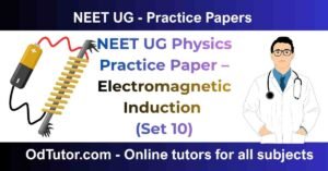
NEET UG Physics Practice Paper – Electromagnetic Induction (Set 10)
Posted By
odadmin
April 15, 2026
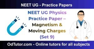
NEET UG Physics Practice Paper – Magnetism & Moving Charges (Set 9)
Posted By
odadmin
April 13, 2026
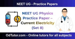
NEET UG Physics Practice Paper – Current Electricity (Set 8)
Posted By
odadmin
April 10, 2026
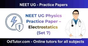
NEET UG Physics Practice Paper – Electrostatics (Set 7)
Posted By
odadmin
April 3, 2026
NEET UG Physics Practice Paper – Part 6 (Modern Physics)
Posted By
odadmin
April 2, 2026
NEET UG – Physics Practice Paper – Thermodynamics (Part 5)
Posted By
odadmin